Recently, relying on high-level platforms such as the “Optical Detection Materials and Devices” Shanghai High-level Local University Innovation Team and the Shanghai Engineering Technology Research Center for Optical Detection Materials and Devices, and funded by the National Key Research and Development Program and the key project of the National Natural Science Foundation of China, the team led by Professor Fang Yongzheng and Professor Liu Yufeng from the School of Materials Science and Engineering of SIT, in collaboration with domestic and foreign institutions such as Hangzhou Institute for Advanced Study, University of Chinese Academy of Sciences and the Massachusetts Institute of Technology (MIT) in the United States, has made significant progress in the heteroepitaxy of two-dimensional semiconductor materials.
With the continuous growth of application demand in the field of high-performance detection technology in China, higher requirements are put forward for new optical detection materials. As one of the core materials of optical detection technology, heteroepitaxial semiconductor materials show broad application prospects because of their excellent photoelectric properties. However, limited by lattice matching, the heteroepitaxy of these materials on a single substrate often faces a high lattice strain, resulting in decreased interface quality, increased crystal defects, and many “stuck neck” technologies. At the same time, expensive semiconductor equipment and complex semiconductor process technology limit its wide application.
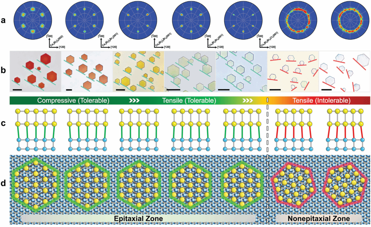
The research team successfully realized the high-oriented epitaxy growth of 2D semiconductor monocrystals on C-plane sapphire substrate by using the “in-plane adaptive heteroepitaxy” strategy. By rotating the crystal orientation at 30°, the compressive stress and tensile stress can be effectively regulated to achieve the tolerance of strain, and the controllable interfacial strain can be formed between heteroepitaxial single crystals with different lattice constants and sapphire substrate. More importantly, the optical detector based on the heteroepitaxial material shows better optical detection performance than the non-epitaxial device.

FIG. 1 Orientation relationship, interfacial strain and lattice matching of semiconductor single crystal during heteroepitaxial growth
The relevant results were published in the top journal Advanced Materials (2024, 2413852, 1-11, impact factor: 27.4) on December 4, 2024, titled “In-Plane Adaptive Heteroepitaxy of 2D Cesium Bismuth Halides with Engineered Bandgaps on c-Sapphire”.

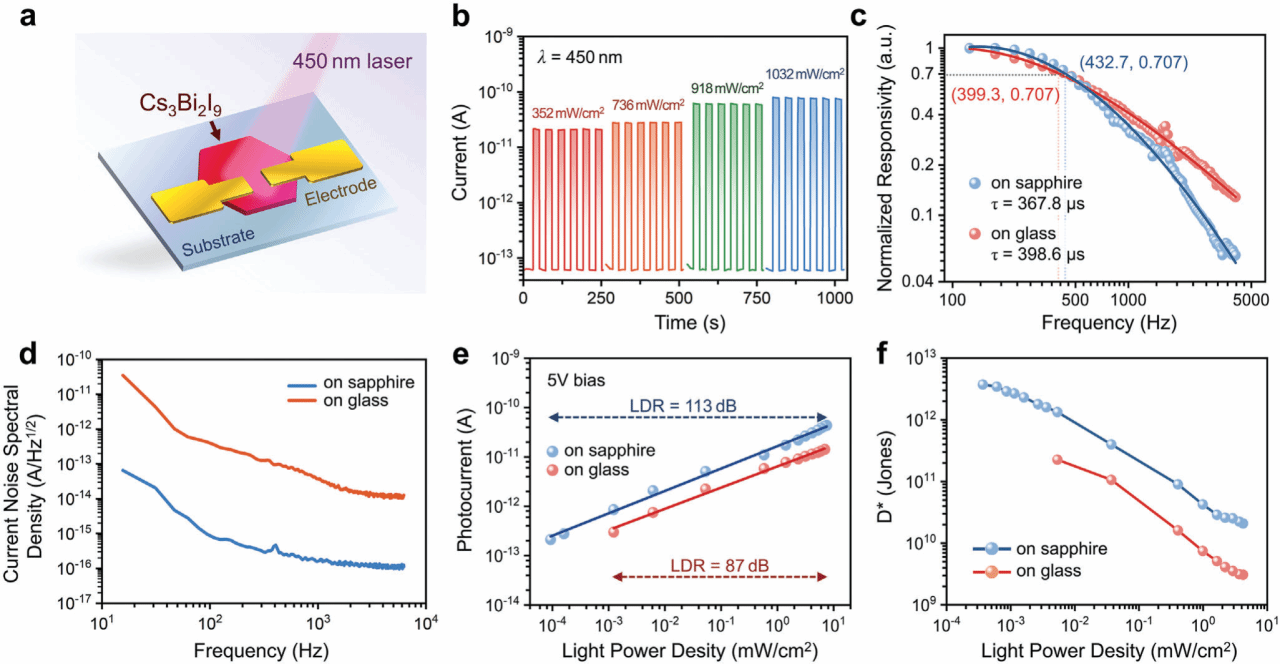
FIG. 2 The photodetector based on epitaxial semiconductor single crystal has significantly improved performance
The experimental results show that the photodetector based on the heteroepitaxy single crystal grown on the C-plane sapphire substrate has a response time of 367.8 μs, a detection rate of 3.7×10¹² Jones and a linear dynamic range (LDR) of 113 dB under laser irradiation at 450 nm wavelength, which is much higher than the traditional glass substrate devices. In addition, the photodetector remains stable in multiple switching cycles and long testing time, showing excellent operational reliability and long device life, providing a new experimental method and theoretical support for the heteroepitaxy growth of new semiconductor materials and its device applications.
Source: School of Materials Science and Engineering

